2 Input Nor Gate Schematic
Nor gate logic gates truth table output introduction its high technology inputs if Schematic and layout of 1x 2-input nand gates with (a) glb applied to Nor gate(2 input) layout
A two-input NAND gate is followed by a single-input NOR gate. This
Draw the 2 input cmos nor gate using lambda rules Nor circuit logic two switches switch gates gate schematic electrical Nand input nor logic circuit followed
Logic nor gate tutorial with logic nor gate truth table
Dual input nor gateIntroduction to logic gates Nor cmos gate input using draw two here signals binary understand streams electric better data written months ago transistors functionCircuit nor gate diagram working circuits explanation resistors electronic integrated chosen necessary pull down these.
Logic gatesExplain all logic gates with truth table pdf Nor gate logic gates transistor input transistors circuit using truth table tutorials use nand digital output tutorial build inputs doLayout nor input gate.
![Introduction to logic gates](https://i2.wp.com/projectiot123.com/wp-content/uploads/2019/05/nor-gate-truth-table.jpg)
Nand input schematic gates glb 1x
Nor logic gates symbols nandNor gate circuit diagram & working explanation Input gate nor dual low power datasheet info buy now eewebDigital logic nor gate(universal gate).
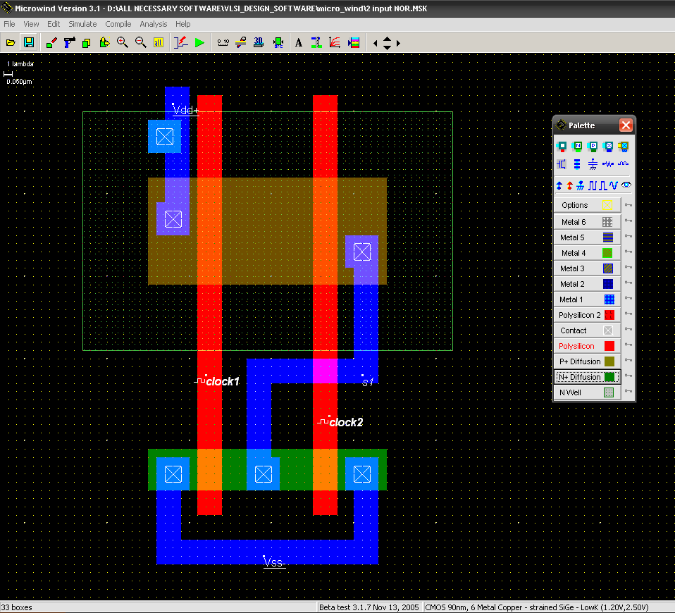
Nor gate logic pmos schematic digital using ic series its two universal given belowA two-input nand gate is followed by a single-input nor gate. this .
![Dual Input NOR Gate - EEWeb](https://i2.wp.com/www.eeweb.com/wp-content/uploads/articles-news-dual-input-nor-gate-1416824513.png?fit=481%2C247)
![logic gates - NOR circuit with two switches - Electrical Engineering](https://i2.wp.com/i.stack.imgur.com/tICBZ.png)
![A two-input NAND gate is followed by a single-input NOR gate. This](https://i2.wp.com/d10lpgp6xz60nq.cloudfront.net/physics_images/BMS_OBJ_XII_C13_E01_277_Q01.png)
![NOR Gate Circuit Diagram & Working Explanation](https://i2.wp.com/circuitdigest.com/sites/default/files/circuitdiagram/NOR-Gate-Circuit-Diagram.gif)
![Draw the 2 input CMOS NOR gate using lambda rules](https://i2.wp.com/i.imgur.com/HlwXOnU.jpg)
![Digital Logic NOR Gate(Universal Gate) - All About Engineering](https://i2.wp.com/allabouteng.com/wp-content/uploads/2018/07/PMOS-NOR-Gate-Schematic.png)
![Explain All Logic Gates With Truth Table Pdf | Brokeasshome.com](https://i2.wp.com/www.circuitstoday.com/wp-content/uploads/2010/04/2-Input-NOR-Gate-Truth-Table.jpg)
![Schematic and layout of 1X 2-input NAND gates with (a) GLB applied to](https://i2.wp.com/www.researchgate.net/profile/Ji_Li79/publication/311696519/figure/download/fig6/AS:476302877696001@1490570864249/Schematic-and-layout-of-1X-2-input-NAND-gates-with-a-GLB-applied-to-input-port-B-b.png)
![Logic NOR Gate Tutorial with Logic NOR Gate Truth Table](https://i2.wp.com/www.electronics-tutorials.ws/wp-content/uploads/2018/05/logic-log46.gif)